Tuning graphene film so it sheds water
The arc bobs against a god. Windshields that shed water so effectively that they don’t need wipers. Ship hulls so slippery that they glide through the water more efficiently than ordinary hulls.
These are some of the potential applications for graphene, one of the hottest new materials in the field of nanotechnology, raised by the research of James Dickerson, assistant professor of physics at Vanderbilt.
Dickerson and his colleagues have figured out how to create a freestanding film of graphene oxide and alter its surface roughness so that it either causes water to bead up and run off or causes it to spread out in a thin layer.
“Graphene films are transparent and, because they are made of carbon, they are very inexpensive to make,” Dickerson said. “The technique that we use can be rapidly scaled up to produce it in commercial quantities.”
His approach is documented in an article published online by the journal ACSNano on Nov. 26.
Graphene is made up of sheets of carbon atoms arranged in rings –d> something like molecular chicken wire. Not only is this one of the thinnest materials possible, but it is 10 times stronger than steel and conducts electricity better at room temperature than any other known material. Graphene’s exotic properties have attracted widespread scientific interest, but Dickerson is one of the first to investigate how it interacts with water.
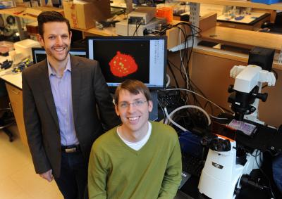
 Physicist James Dickerson, left, and graduate student Saad Hasan (Photo by Daniel Dubois) Physicist James Dickerson, left, and graduate student Saad Hasan (Photo by Daniel Dubois) |
Many scientists studying graphene make it using a dry method, called “mechanical cleavage,” that involves rubbing or scraping graphite against a hard surface. The technique produces sheets that are both extremely thin and extremely fragile. Dickerson’s method can produce sheets equally as thin but considerably stronger than those made by other techniques. It is already used commercially to produce a variety of different coatings and ceramics. Known as electrophoretic deposition, this “wet” technique combines an electric field within a liquid medium to create nanoparticle films that can be transferred to another surface. |
Dickerson and his colleagues found that they could change the manner in which the graphene oxide particles assemble into a film by varying the pH of the liquid medium and the electric voltage used in the process. One pair of settings lay down the particles in a “rug” arrangement that creates a nearly atomically smooth surface. A different pair of settings causes the particles to clump into tiny “bricks” forming a bumpy and uneven surface. The researchers determined that the rug surface causes water to spread out in a thin layer, while the brick surface causes water to bead up and run off.
Dickerson is pursuing an approach that could create film that enhances these water-associated properties, making them even more effective at either spreading out water or causing it to bead up and run off. There is considerable academic and commercial interest in the development of coatings with these enhanced properties, called super-hydrophobic and super-hydrophilic. Potential applications range from self-cleaning glasses and clothes to antifogging surfaces to corrosion protection and snow-load protection on buildings. However, effective, low-cost and durable coatings have yet to make it out of the laboratory.
Dickerson’s idea is to apply his basic procedure to “fluorographene” – a fluorinated version of graphene that is a two-dimensional version of Teflon – recently produced by Kostya S. Novoselov and Andre K. Geim at the University of Manchester, who received the 2010 Nobel Prize for the discovery of graphene. Normal fluorographene under tension should be considerably more effective in repelling water than graphene oxide. So there is a good chance a “brick” version and a “rug” version would have extreme water-associated effects, Dickerson figures.
Graduate students Saad Hasan, John Rigueur, Robert Harl and Alex Krejci, postdoctoral research scientist Isabel Gonzalo-Juan and Associate Professor of Chemical and Biomolecular Engineering Bridget R. Rogers contributed to the research, which was funded by a Vanderbilt Discovery grant and by the National Science Foundation.
Contact: David F. Salisbury david.salisbury@vanderbilt.edu 615-343-6803 Vanderbilt University
Engineered cells could usher in programmable cell therapies
Researchers at BWH have engineered cells that could solve one of the key challenges associated with the procedure: Control of the cells and their microenvironment following transplantation.
Boston, MA – In work that could jumpstart the promising field of cell therapy, in which cells are transplanted into the body to treat a variety of diseases and tissue defects, researchers at Brigham and Women’s Hospital (BWH) have engineered cells that could solve one of the key challenges associated with the procedure: control of the cells and their microenvironment following transplantation.
In the work, reported in the journal Biomaterials on January 26, the team reports creating tiny internal depots within human mesenchymal adult stem cells, which among other functions are key to the generation of several tissues. These depots can slowly release a variety of agents to influence the behavior of not only the cells containing the depots, but also those close to them and even much farther away. The team demonstrated this by prompting mesenchymal stem cells to differentiate into the cells that make bone.
“This work could allow programmable cell therapies where the cell or the agent is the therapeutic,” says Jeffrey Karp, leader of the work and co-director of the Center for Regenerative Therapeutics (ReGen Rx) at BWH. “For example, depots containing specific agents could enhance cell survival or expression of a particular growth factor. Cells could also be used as a delivery vehicle to shuttle drugs to target tissues that may be useful to accelerate tissue regeneration, or to deliver chemotherapeutics to tumors while minimizing systemic side effects.”
Caption: Researchers at Brigham and Women’s Hospital have engineered human mesenchymal adult stem cells (one cell shown, in red) to contain tiny depots (green) that can influence the behavior of the cells and those surrounding them, including their survival, differentiation, or production of a therapeutic protein. Left is Jeffrey Karp, co-director of the Center for Regenerative Therapeutics at Brigham & Women’s Hospital, right is James A. Ankrum, co-first author on the paper and an HST graduate student. Not shown: Debanjan Sarkar, also a co‑first author of the paper, now at the University of Buffalo. Credit: Photo by Donna Coveney. Usage Restrictions: None.
Caption: Researchers at Brigham and Women’s Hospital have engineered human mesenchymal adult stem cells (one cell shown, in red) to contain tiny depots (green) that can influence the behavior of the cells and those surrounding them, including their survival, differentiation, or production of a therapeutic protein. Credit: Image courtesy Karp lab, Brigham and Women’s Hospital. Usage Restrictions: None. |
Toward Cell Therapy
“Ten to fifteen years from now, people will visit cell infusion centers to receive routine therapy for multiple diseases and tissue defects,” predicts Karp, who also holds appointments through Harvard Medical School, Harvard Stem Cell Institute, and the Harvard-MIT Division of Health Sciences and Technology (HST). For example, a person who has had a heart attack could be infused with cells that could help stimulate regeneration of new heart cells to replace those that have died and prevent eventual heart failure. Today, however, there is only one cell therapy that has saved tens of thousands of lives: bone marrow transplantation. In this procedure healthy blood stem cells home in to the bone marrow to regenerate the blood system of cancer patients following bone marrow ablation through chemotherapy or radiation. One of the reasons for the lack of success of other cell therapies is the inability to control the cells and the host’s response following transplantation, says Karp. “We can exhibit exquisite control over cells in a [laboratory] dish—we can get them to do whatever we want. But when we transplant them into the body, their fate and function are at the mercy of the biological milieu. We typically lose complete control and this prevents us from achieving the promise of cell therapy.” There are ways to get around this problem, but they have limitations. For example, cells can be put on a scaffold or biomaterial that releases drugs or other agents that affect their behavior. The cells, however, have to stay in close proximity to the material to be impacted by the agents. Cells can also be genetically modified with viruses to produce agents that will influence their behavior, but this has potential safety concerns. Natural Inspiration The Karp team was inspired by the natural ability of many proteins and other agents to be transported in and out of cells. They already knew that cells could internalize the tiny synthetic particles used in the controlled delivery of drugs—could these particles be used in cell therapy? To find out, the researchers developed biodegradable particles about ten times smaller than a mesenchymal stem cell (MSC). |

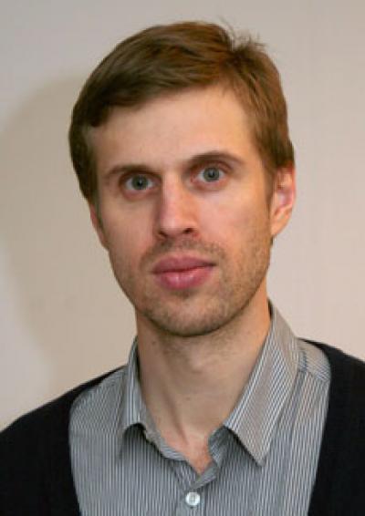
They loaded these particles with a dye, placed them near living MSCs, and found that the cells did indeed internalize them without immediately spitting them out. “Initially, this was a major challenge,” comments James A. Ankrum, co-first author on the paper and an HST graduate student. “The particles needed to be small enough for the cells to internalize, yet large enough to prevent being shed by the cell.” The dye was observed to seep from the tiny particle depots to the outside of the cell through the cell membrane over a period of several days.
Next, they replaced the dye with an agent known to spur MSCs to differentiate into osteoblasts, the cells that make bone. They found that not only did MSCs containing the depots differentiate into osteoblasts, but so did MSCs without depots that were nearby and even much further away. “We demonstrated that the fate of particle-carrying cells could be controlled, as well as the fates of neighboring and distant cells,” says Debanjan Sarkar, co-first author of the paper and now a professor at the University of Buffalo.
Additional authors are Grace S. L. Teo of HST and Christopher V. Carman of Beth Israel Deaconess Hospital.
To date the team has demonstrated the engineered cells in laboratory systems designed to mimic the body. They are in the process of translating the work to animals. “If it works in vivo, it could have a significant impact globally on cell therapy,” says Karp, whose team has filed for a patent on the work.
###
This work was funded by the National Institutes of Health, the American Heart Association, and the National Science Foundation.
Contact: Holly Brown-Ayers hbrown-ayers@partners.org 617-534-1603 Brigham and Women’s Hospital
NIST technique controls sizes of nanoparticle clusters for EHS studies
The same properties that make engineered nanoparticles attractive for numerous applications—small as a virus, biologically and environmentally stabile, and water-soluble—also cause concern about their long-term impacts on environmental health and safety (EHS). One particular characteristic, the tendency for nanoparticles to clump together in solution, is of great interest because the size of these clusters may be key to whether or not they are toxic to human cells. Researchers at the National Institute of Standards and Technology (NIST) have demonstrated for the first time a method for producing nanoparticle clusters in a variety of controlled sizes that are stable over time so that their effects on cells can be studied properly.*
In their tests, the NIST team made samples of gold, silver, cerium oxide and positively-charged polystyrene nanoparticles and suspended them separately in cell culture medium, allowing clumping to occur in each. They stopped the clumping by adding a protein, bovine serum albumin (BSA), to the mixtures. The longer the nanoparticles were allowed to clump together, the larger the size of the resulting cluster. For example, a range of clustering times using 23 nanometer silver nanoparticles produced a distribution of masses between 43 and 1,400 nanometers in diameter. Similar size distributions for the other three nanoparticle types were produced using this method.

Caption: Transmission electron micrograph of gold nanoparticles clustering in solution. The distance between the two red arrows is approximately 280 nanometers, some 200 times smaller than the diameter of a human hair. The individual nanoparticles are approximately 15 nanometers in diameter, about the distance across 40 side-by-side sodium atoms. Credit: A. Keene, US Food and Drug Administration. Usage Restrictions: None. |
The researchers learned that using the same “freezing times”—the points at which BSA was added to halt the process—yielded consistent size distributions for all four nanoparticle types. Additionally, all of the BSA-controlled dispersions remained stable for 2-3 days, which is sufficient for many toxicity studies.
Having successfully shown that they could control the production of nanoparticle clumps of different sizes, the researchers wanted next to prove that their creations could be put to work. Different-sized silver nanoparticle clusters were mixed with horse blood in an attempt to study the impact of clumping size on red blood cell toxicity. The presence of hemoglobin, the iron-based molecule in red blood cells that carries oxygen, would tell researchers if the cells had been lysed (broken open) by silver ions released into the solution from the clusters. |
In turn, measuring the amount of hemoglobin in solution for each cluster size would define the level of toxicity—possibly related to the level of silver ion release—for that specific average size.
What the researchers found was that red blood cell destruction decreased as cluster size increased. They hypothesize that large nanoparticle clusters dissolve more slowly than small ones, and therefore, release fewer silver ions into solution.
In the future, the NIST team plans to further characterize the different cluster sizes achievable through their production method, and then use those clusters to study the impact on cytotoxicity of coatings (such as polymers) applied to the nanoparticles.
###
* J.M. Zook, R.I. MacCuspie, L.E. Locascio, M.D. Halter and J.T. Elliott. Stable nanoparticle aggregates/agglomerates of different sizes and the effect of their size on hemolytic cytotoxicity. Nanotoxicology, published online Dec. 13, 2010 (DOI: 10.3109/17435390.2010.536615).
Contact: Michael E. Newman michael.newman@nist.gov 301-975-3025 National Institute of Standards and Technology (NIST)
A new record for Tyndall’s revolutionary microchip technology VIDEO
Last February, Nature Nanotechnology announced the development at UCC’s Tyndall National Institute of the world’s first junctionless transistor. The transistor is the building block of the microchip and the breakthrough by Professor Jean-Pierre Colinge, was greeted by the semiconductor industry as a major advance. Now, Professor Colinge is back in the news with a transistor that is reduced again by a factor of twenty. To put in it context, his latest innovation is 2000 times smaller than a strand of human hair, 30 per cent more energy efficient than existing transistors and gives a better performance than transistors now on the market! With up to two billion transistors on a single microchip, the latest breakthrough will help to drive more simple manufacturing processes and is again being viewed as a significant leap forward. Professor Colinge explains:
TEXT and VIDEO CREDIT: UCCIreland
New nanomaterials unlock new electronic and energy technologies
Atom-thick sheets unlock future technologies
A new way of splitting layered materials to give atom thin “nanosheets” has been discovered. This has led to a range of novel two-dimensional nanomaterials with chemical and electronic properties that have the potential to enable new electronic and energy storage technologies. The collaborative* international research led by the Centre for Research on Adaptive Nanostructures and Nanodevices (CRANN), Trinity College Dublin, Ireland, and the University of Oxford has been published in this week’s Science.
The scientists have invented a versatile method for creating these atom thin nanosheets from a range of materials using common solvents and ultrasound, utilising devices similar to those used to clean jewellery. The new method is simple, fast, and inexpensive, and could be scaled up to work on an industrial scale.
“Of the many possible applications of these new nanosheets, perhaps the most important are as thermoelectric materials. These materials, when fabricated into devices, can generate electricity from waste heat. For example, in gas-fired power plants approximately 50% of energy produced is lost as waste heat while for coal and oil plants the figure is up to 70%. However, the development of efficient thermoelectric devices would allow some of this waste heat to be recycled cheaply and easily, something that has been beyond us, up until now,” explained Professor Jonathan Coleman, Principal Investigator at CRANN and the School of Physics, Trinity College Dublin who led the research along with Dr Valeria Nicolosi in the Department of Materials at the University of Oxford.

Prof Jonathan Coleman (left) pictured with CRANN Director, Prof John Boland |
This research can be compared to the work regarding the two-dimensional material graphene, which won the Nobel Prize in 2010. Graphene has generated significant interest because when separated into individual flakes, it has exceptional electronic and mechanical properties that are very different to those of its parent crystal, graphite. However, graphite is just one of hundreds of layered materials, some of which may enable powerful new technologies. |
Coleman’s work will open up over 150 similarly exotic layered materials – such as Boron Nitride, Molybdenum disulfide, and Bismuth telluride – that have the potential to be metallic, semiconducting or insulating, depending on their chemical composition and how their atoms are arranged. This new family of materials opens a whole range of new “super” materials.
For decades researchers have tried to create nanosheets from layered materials in order to unlock their unusual electronic and thermoelectric properties. However, previous methods were time consuming, laborious or of very low yield and so unsuited to most applications.
“Our new method offers low-costs, a very high yield and a very large throughput: within a couple of hours, and with just 1 mg of material, billions and billions of one-atom-thick nanosheets can be made at the same time from a wide variety of exotic layered materials,” explained Dr Nicolosi, from the University of Oxford.
These new materials are also suited for use in next generation batteries – “supercapacitors” – which can deliver energy thousands of times faster than standard batteries, enabling new applications such as electric cars. Many of these new atomic layered materials are very strong and can be added to plastics to produce super-strong composites. These will be useful in a range of industries from simple structural plastics to aeronautics.
###
*Other collaborators in the research were Korea University, Texas A &M University, Imperial College London
*The research paper titled ‘Two-dimensional nanosheets produced by liquid exfoliation of layered materials’, is published in the 4 February edition of the journal Science.
Contact: Professor Jonathan Coleman colemaj@tcd.ie 003-538-778-34917 Trinity College Dublin
Engineers grow nanolasers on silicon, pave way for on-chip photonics
Berkeley – Engineers at the University of California, Berkeley, have found a way to grow nanolasers directly onto a silicon surface, an achievement that could lead to a new class of faster, more efficient microprocessors, as well as to powerful biochemical sensors that use optoelectronic chips.
They describe their work in a paper to be published Feb. 6 in an advanced online issue of the journal Nature Photonics.
“Our results impact a broad spectrum of scientific fields, including materials science, transistor technology, laser science, optoelectronics and optical physics,” said the study’s principal investigator, Connie Chang-Hasnain, UC Berkeley professor of electrical engineering and computer sciences.
The increasing performance demands of electronics have sent researchers in search of better ways to harness the inherent ability of light particles to carry far more data than electrical signals can. Optical interconnects are seen as a solution to overcoming the communications bottleneck within and between computer chips.
Because silicon, the material that forms the foundation of modern electronics, is extremely deficient at generating light, engineers have turned to another class of materials known as III-V (pronounced “three-five”) semiconductors to create light-based components such as light-emitting diodes (LEDs) and lasers.

Caption: Shown is a schematic (left) and various scanning electron microscope images of nanolasers grown directly on a silicon surface. The achievement could lead to a new class of optoelectronic chips. Credit: Connie Chang-Hasnain Group. Usage Restrictions: Must include credit with use.
Caption: The unique structure of the nanopillars grown by UC Berkeley researchers strongly confines light in a tiny volume to enable subwavelength nanolasers. Images on the left and top right show simulated electric field intensities that describe how light circulates helically inside the nanopillars. On the bottom right is an experimental camera image of laser light from a single nanolaser. Credit: Connie Chang-Hasnain Group. Usage Restrictions: Must include credit with use. |
But the researchers pointed out that marrying III-V with silicon to create a single optoelectronic chip has been problematic. For one, the atomic structures of the two materials are mismatched.
“Growing III-V semiconductor films on silicon is like forcing two incongruent puzzle pieces together,” said study lead author Roger Chen, a UC Berkeley graduate student in electrical engineering and computer sciences. “It can be done, but the material gets damaged in the process.” Moreover, the manufacturing industry is set up for the production of silicon-based materials, so for practical reasons, the goal has been to integrate the fabrication of III-V devices into the existing infrastructure, the researchers said. “Today’s massive silicon electronics infrastructure is extremely difficult to change for both economic and technological reasons, so compatibility with silicon fabrication is critical,” said Chang-Hasnain. “One problem is that growth of III-V semiconductors has traditionally involved high temperatures – 700 degrees Celsius or more – that would destroy the electronics. Meanwhile, other integration approaches have not been scalable.” The UC Berkeley researchers overcame this limitation by finding a way to grow nanopillars made of indium gallium arsenide, a III-V material, onto a silicon surface at the relatively cool temperature of 400 degrees Celsius. “Working at nanoscale levels has enabled us to grow high quality III-V materials at low temperatures such that silicon electronics can retain their functionality,” said Chen. The researchers used metal-organic chemical vapor deposition to grow the nanopillars on the silicon. “This technique is potentially mass manufacturable, since such a system is already used commercially to make thin film solar cells and light emitting diodes,” said Chang-Hasnain. |

Once the nanopillar was made, the researchers showed that it could generate near infrared laser light – a wavelength of about 950 nanometers – at room temperature. The hexagonal geometry dictated by the crystal structure of the nanopillars creates a new, efficient, light-trapping optical cavity. Light circulates up and down the structure in a helical fashion and amplifies via this optical feedback mechanism.
The unique approach of growing nanolasers directly onto silicon could lead to highly efficient silicon photonics, the researchers said. They noted that the miniscule dimensions of the nanopillars – smaller than one wavelength on each side, in some cases – make it possible to pack them into small spaces with the added benefit of consuming very little energy
“Ultimately, this technique may provide a powerful and new avenue for engineering on-chip nanophotonic devices such as lasers, photodetectors, modulators and solar cells,” said Chen.
“This is the first bottom-up integration of III-V nanolasers onto silicon chips using a growth process compatible with the CMOS (complementary metal oxide semiconductor) technology now used to make integrated circuits,” said Chang-Hasnain. “This research has the potential to catalyze an optoelectronics revolution in computing, communications, displays and optical signal processing. In the future, we expect to improve the characteristics of these lasers and ultimately control them electronically for a powerful marriage between photonic and electronic devices.”
###
The Defense Advanced Research Projects Agency and a Department of Defense National Security Science and Engineering Faculty Fellowship helped support this research.
Contact: Sarah Yang scyang@berkeley.edu 510-643-7741 University of California – Berkeley
Taming carbon nanotubes
Carbon nanotubes have many attractive properties, and their structure and areas of application can be compared with those of graphene, the material for whose discovery the most recent Nobel Prize was awarded. In order to be able to exploit these properties, however, it is necessary to have full control of the manufacturing process. Scientists at the University of Gothenburg are closing in on the answer.
“Our results show that the metal particles that form the basis of the manufacture of carbon nanotubes must have a certain minimum size, in order for growth to start and to continue. It is also probable that the particles are in liquid form at a manufacturing temperature of around 800 °C, even though the metals used may have much higher melting points”, says Anders Börjesson from the Department of Physics at the University of Gothenburg.
The scientists have used various computer models to study in detail properties that are difficult or impossible to examine in experimental conditions. Only when we fully understand the manufacturing process will we be able to exploit this material fully.
The diameter of the nanotubes is of the order of one billionth of a metre, and they can be as thin as a single carbon layer. The length of the tubes, in contrast, can extend from the nanometre scale up to several decimetres. Carbon nanotubes can be regarded, quite simply, as thin threads of pure carbon, whose length can be a billion times greater than their thickness.
Caption: This is Anders Börjesson of the University of Gothenburg. Credit: Matilda Hagberg. Usage Restrictions: None. |
Interest for nanotubes is based on their outstanding properties: they are among the strongest materials known and have extremely high conductivity for both electric current and heat.
The strength can be used to reinforce other materials, just as the strength of glass and carbon fibres is used in plastics, and steel reinforcement is used in concrete. Carbon nanotubes, however, would enable plastics to be manufactured that are ten times stronger than the strongest materials available today. Such materials could be used not only in exclusive sports equipment but also in the construction of buildings that appear to come from science fiction: a lift between the Earth and space could be anchored using a material based on nanotubes. The carbon nanotubes may also replace other material when it comes to conducting very high electrical currents, since they do not become hot, nor do they catch fire. Certain nanotubes have semiconducting properties and could be used to build nanoelectronic circuits, giving much smaller and faster processors to be used in computers. |
One way of combining the strength and electrical properties of the carbon nanotubes would be to mix them with polymer material, and by weaving threads that also contain electronic circuits. It would be possible, for example, to weave instruments for monitoring heart function directly into clothes.
###
The thesis In Silco Studies of Carbon Nanotubes and Metal Clusters (Beräkningsstudier av kolnanorör och metallkluster) has been successfully defended. Supervisor: Professor Kim Bolton. The research has been a collaboration between the University of Gothenburg and the University of Borås.
Contact: Anders Börjesson anders.borjesson@physics.gu.se 46-031-786-9143 University of Gothenburg
Keck Foundation funds work on tiny, implantable computers to restore lost brain functions
If successful, the devices would bridge impaired nerve connections and promote brain recovery from injury or disease.
Tiny, implantable computers that would restore brain function lost to disease or injury is the goal of University of Washington research recently funded by a $1 million, three-year grant from the W.M. Keck Foundation.
The UW has made significant progress in neural engineering – the study of communication and control between biological and machine systems. The Keck project is the next step in advancing the technology of miniature devices developed at the UW to record from and stimulate the brain, spinal cord and muscles.
The principal investigator on the Keck Foundation grant is Dr. Eberhard E. Fetz, UW professor of physiology and biophysics and a core staff researcher at the Washington National Primate Research Center. He and his colleagues have successfully deployed tiny, battery-powered implantable brain-computer interfaces called neurochips in animals.
The neurochip can record nerve cell activity in one part of the brain, process this activity and then stimulate cells in another brain region. The battery-powered device operates continuously during free behavior. When primates carry out their usual daily activities – socializing, climbing, eating, and exploring – their brains can learn to exploit these new resources under normal behavioral conditions.

Caption: Dr. Eberhard Fetz at the University of Washington in Seattle is principal investigator on a W.M. Keck Foundation grant to develop tiny, implantable computers to restore brain functions lost to injury or disease. Credit: Leila Gray. Usage Restrictions: None. |
One potential clinical application is to bridge lost biological connections. For example, the researchers have shown that monkeys can learn to bypass an anesthetic block in the nerves of the arm and to activate temporarily paralyzed muscles with activity of cortical neurons. In some ways the device acts as a volition processor, tapping into signals representing the will to move and using them to stimulate the paralyzed muscles to reach targets.
“Using an implantable computer interface to implement novel interactions between brain sites opens many fundamentally new research directions,” Fetz said, “depending on the site of recording and stimulation, and how these signals are processed and transformed.” He explained that a second application is to promote neural plasticity, which could strengthen connections and allow some of the brain’s functions to be rescued when impaired. |
This happens naturally when people recover the ability to move or speak again after a stroke or brain injury. The bidirectional brain computer interface could facilitate this recovery and exploit the brain’s innate talent for re-organizing itself as it heals.
“We expect that the recurrent type of brain computer interface we are trying to develop,” he added, “will eventually have numerous clinical applications for bridging damaged biological pathways and strengthening weak neural connections.” For example, signals from the motor-control regions of the brain can be used to stimulate parts of the spinal cord to evoke coordinated movements. This would create connections that could replace lost pathways between the brain and spinal cord, a loss that occurs with strokes and spinal cord injuries.
Many labs around the world are working on brain-computer interfaces that convert neural activity to control of external devices such as prosthetic limbs or computer cursors. What makes the recently funded project unusual is that its scientists are developing a recurrent implantable device that would interact bidirectionally with the brain. By operating autonomously and continuously, without the need for connection to external instrumentation, it would facilitate long-term behavioral adaptation and plasticity.
The proposed research plans to develop this new paradigm to promote restoration of brain, spine, and muscle function. The work could eventually lead to miniaturized electrical and biological interfaces that operate around the clock on a small amount of power while the wearer goes about his or her usual activities, according to Fetz. He added that, if successful, this implantable technology would advance the ability of subjects to effectively control a brain computer interface by allowing long-term adaptation to consistent contingencies, and would open opportunities for the brain to exploit bidirectional interactions with miniature computers. This implementation of continuous reciprocal interaction goes beyond the existing paradigm of using brain signals to control external devices through tethered connections.
As part of the project the team also plans to create a powerful multichannel “Keck Active Electrode Array” with integrated electronics to record and stimulate large numbers of brain sites. This array would operate with electrodes on the surface of the brain and be less invasive than penetrating intracortical electrodes.
To overcome the many technical problems in creating safe, effective devices of this nature and realizing their clinical potential, the project depends on a team of UW experts in different fields.
Dr. Brian Otis, UW assistant professor of electrical engineering, has extensive experience in wireless sensors and in designing extremely small radios that can be incorporated into other devices. He is also an expert in bioelectronics and the processing of signals with minimal power. His group will design and miniaturize the low power circuitry for the computer and the signal amplifiers, and will work toward harvesting energy to operate the device, perhaps from the body’s own heat or muscle activity.
Dr. Babak Parviz, the UW McMorrow Innovation Associate Professor of Electrical Engineering, has skill in the fabrication of micro- and nano-scale tools, self-assembled biocompatible machinery, and sensors for detecting very faint signals. His group will create the specialized electrode arrays for recording and stimulation, and will help integrate the miniature electronic systems used in the project.
Dr. Jeffrey Ojemann, UW professor of neurological surgery, has expanded his father’s original studies on mapping of the human brain to identify critical areas for movement, language, memory and other functions prior to epilepsy surgery. He will bring his extensive knowledge of functional brain mapping and clinical recording of signals from the human brain to the project. He will help design and test the custom computer-enabled electrode arrays for potential applications to patient care.
Among the engineering and health issues the team will be addressing are integrating the electronics with the electrode array and making it small enough, finding a reliable source of the low power necessary to operate the system, evaluating any hazards the device might pose or serious long-term side effects, and developing biomaterials that won’t cause irritation or be rejected, as well as meeting other safety, performance, and acceptability criteria.
“We are extremely grateful to the Keck Foundation for supporting this highly ambitious endeavor,” Fetz said. “Looking ahead, we can anticipate that future innovations in nanotechnology, computers and brain science will advance this effort beyond the current state of the art. The grant allows us to be poised to incorporate these advances into the development of more powerful recurrent brain computer interfaces. We expect that these devices will have numerous applications in basic neuroscience research and as well as in clinical care.”
###
About the W.M. Keck Foundation
Based in Los Angeles, the W. M. Keck Foundation was established in 1954 by the late W. M. Keck, founder of the Superior Oil Company. The Foundation’s grant making is focused primarily on pioneering efforts in the areas of medical research, science and engineering and undergraduate education. The Foundation also maintains a Southern California Grant Program that provides support for the Los Angeles community, with a special emphasis on children and youth. For more information, please visit www.wmkeck.org
About UW Medicine
UW Medicine trains health professionals and medical scientists, conducts research to improve health and prevent disease, and provides primary and specialty care to patients throughout Seattle/King County and the WWAMI (Washington, Wyoming, Alaska, Montana and Idaho) region. UW Medicine includes Harborview Medical Center, UW Medical Center, Northwest Hospital & Medical Center, UW Neighborhood Clinics, UW School of Medicine, UW Physicians, and Airlift Northwest. UW Medicine also shares in the ownership and governance of the Seattle Cancer Care Alliance with Seattle Children’s Hospital and Fred Hutchinson Cancer Research Center and shares in the ownership of Children’s University Medical Group with Children’s Hospital.
UW Medicine has major academic and service affiliations with Seattle Children’s Hospital, Fred Hutchinson Cancer Research Center, the VA Puget Sound Health Care System in Seattle, and the VA Hospital in Boise. The UW School of Medicine has been ranked No. 1 in the nation in primary-care training for the past 17 years by U.S. News & World Report and is the top public institution for receipt of biomedical research funding from the National Institutes of Health, and second among all institutions, public and private, for NIH funding. UW Medicine’s 2,400 faculty physicians and nearly 5,000 volunteer and part-time faculty include four Nobel Laureates, 32 members of the National Academy of Sciences, five members of the National Academy of Engineering and 33 members of the Institute of Medicine. For more information, visit www.uwmedicine.org
Contact: Leila Gray leilag@u.washington.edu 206-685-0381 University of Washington
…Listen to this article in MP3 Format When worms stick together and swim on thin water, what happens and why does it matter?
Nematodes, microscopic worms, are making engineers look twice at their ability to exhibit the “Cheerios effect” when they move in a collective motion.
These parasites will actually stick together like Cheerios swimming in milk in a cereal bowl after a chance encounter “due to capillary force.” This observation has made Virginia Tech engineers speculate about the possible impacts on the study of biolocomotion.
Their work appears in the journal, Soft Matter, a publication of the Royal Society of Chemistry, the week of Feb. 7. Soft Matter is the premier journal in the ongoing multidisciplinary work between physics, material science, and biology.
Two Harvard physicists first defined the Cheerios effect. In 2005, Dominic Vella and Lakshminarayanan Mahadevan wrote an article on this activity, defined by scientists as relating to fluid mechanics, in the Journal of Physics. They cited its usefulness in the study of self-assembly of small structures. Self-assembly is used in the science of nanotechnology.
Dominic Vella who now teaches at the University of Oxford, United Kingdom, collaborated with Sunghwan “Sunny” Jung, an assistant professor of engineering science and mechanics at Virginia Tech, and his student, Sean Gart, of Salem, Va., a senior in engineering science and mechanics, and authored the new paper, “The collective motion of nematodes in a thin liquid layer.”

Caption: Sean Gart, of Salem, Va., a senior in engineering science and mechanics at Virginia Tech, co-authored the new paper, “The collective motion of nematodes in a thin liquid layer.” His adviser is Sunghwan “Sunny” Jung, an assistant professor of engineering science and mechanics at Virginia Tech. Credit: Virginia Tech Photo. Usage Restrictions: The photo may be used with any report or discussion of Sean Gart’s research. |
Their work highlights the behaviors of the nematode Panagrellus redivivus, a creature that feeds on bacteria, in a watery liquid layer that is thinner than a human hair. In this environment the nematodes crawl by creating waves that travel backwards down their body, and the force pushes them forward.
“The inspiration for the project came when we observed the nematodes crawling up the side of their container and sticking together. We knew part of the reason for this behavior was due to the capillary force, the same force that causes Cheerios to stick together in a cereal bowl, but we wanted to see whether or not the nematodes moved faster or more efficiently while stuck together,” Jung and Gart explained. “Thin water refers to the air/liquid interface. Like Cheerios in milk, the nematodes are aggregating on top of the air surface, not on the bulk or on the bottom,” Jung said. |
Gart has been working in Virginia Tech’s Biologically Inspired Fluids Laboratory directed by Jung since last summer. Gart found that the nematodes did not crawl faster or more efficiently while stuck together.
“This is an interesting behavior that has not been studied very widely in the biolocomotion field,” Jung said. “The result implies that nematodes gain neither a mechanical advantage nor disadvantage by being grouped together. The capillary forces merely keep them together after a chance encounter. This result also extends a better understanding of capillary effects in colloidal particles in engineering systems such as pickering emulsions. These emulsions are stabilized by solid particles. An example would be homogenized milk.”
###
Contact: Lynn Nystrom tansy@vt.edu 540-231-4371 Virginia Tech
Hydrogels used to make precise new sensor
WEST LAFAYETTE, Ind. – Researchers are developing a new type of biological and chemical sensor that has few moving parts, is low-cost and yet highly sensitive, sturdy and long-lasting.
The “diffraction-based” sensors are made of thin stripes of a gelatinous material called a hydrogel, which expands and contracts depending on the acidity of its environment.
Recent research findings have demonstrated that the sensor can be used to precisely determine pH – a measure of how acidic or basic a liquid is – revealing information about substances in liquid environments, said Cagri Savran (pronounced Chary Savran), an associate professor of mechanical engineering at Purdue University.
The sensor’s simple design could make it more practical than other sensors in development, he said.
“Many sensors being developed today are brilliantly designed but are too expensive to produce, require highly skilled operators and are not robust enough to be practical,” said Savran, whose work is based at Purdue’s Birck Nanotechnology Center in the university’s Discovery Park.

Caption: This diagram depicts a new type of “diffraction-based” sensor made of thin stripes of a gelatinous material called a hydrogel, which expands and contracts depending on the acidity of its environment. The new type of biological and chemical sensor has few moving parts and works by precisely determining pH, revealing the identity of substances in liquid environments such as water or blood. The microscopic images Credit: Birck Nanotechnology Center, Purdue University. Usage Restrictions: None. |
New findings show the technology is highly sensitive and might be used in chemical and biological applications including environmental monitoring in waterways and glucose monitoring in blood.
“As with any novel platform, more development is needed, but the detection principle behind this technology is so simple that it wouldn’t be difficult to commercialize,” said Savran, who is collaborating with another team of researchers led by Babak Ziaie, a Purdue professor of electrical and computer engineering and biomedical engineering. Findings are detailed in a paper presented during the IEEE Sensors 2010 Conference in November and also published in the conference proceedings. The paper was written by postdoctoral researcher Chun-Li Chang, doctoral student Zhenwen Ding, Ziaie and Savran. The flexible, water-insoluble hydrogel is formed into a series of raised stripes called a “diffraction grating,” which is coated with gold on both the stripe surfaces and the spaces in between. |
The stripes expand and contract depending on the pH level of the environment.
Researchers in Ziaie’s lab fabricated the hydrogel, while Savran’s group led work in the design, development and testing of the diffraction-based sensor.
The sensors work by analyzing laser light reflecting off the gold coatings. Reflections from the stripes and spaces in between interfere with each other, creating a “diffraction pattern” that differs depending on the height of the stripes.
These diffraction patterns indicate minute changes in the movement of the hydrogel stripes in response to the environment, in effect measuring changes in pH.
“By precise measurement of pH, the diffraction patterns can reveal a lot of information about the sample environment,” said Savran, who by courtesy is an associate professor of biomedical engineering and electrical and computer engineering. “This technology detects very small changes in the swelling of the diffraction grating, which makes them very sensitive.”
The pH of a liquid is recorded on a scale from 0 to 14, with 0 being the most acidic and 14 the most basic. Findings showed the device’s high sensitivity enables it to resolve changes smaller than one-1,000th on the pH scale, measuring swelling of only a few nanometers. A nanometer is about 50,000 times smaller than the finest sand grain.
“We know we can make them even more sensitive,” Savran said. “By using different hydrogels, gratings responsive to stimuli other than pH can also be fabricated.”
The work is ongoing.
“It’s a good example of collaborations that can blossom when labs focusing on different research are located next to each other,” Savran said. “Professor Ziaie’s lab was already working with hydrogels, and my group was working on diffraction-based sensors. Hearing about the hydrogels work next door, one of my postdoctoral researchers, Chun-Li Chang thought of making a reflective diffraction grating out of hydrogels.”
###
The Office of Technology Commercialization of the Purdue Research Foundation has filed for U.S. patent protection on the concept.
Contact: Emil Venere venere@purdue.edu 765-494-4709 Purdue University
